Salience Labs goes all-in on all-optical networking with photonics switches for AI infrastructure

Oxfordshire-headquartered Salience Labs is hoping to tap into a market that some analysts say could represent as much of a leap in computing power as the emerging field of quantum itself does.
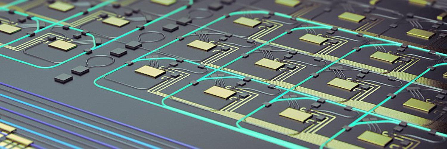
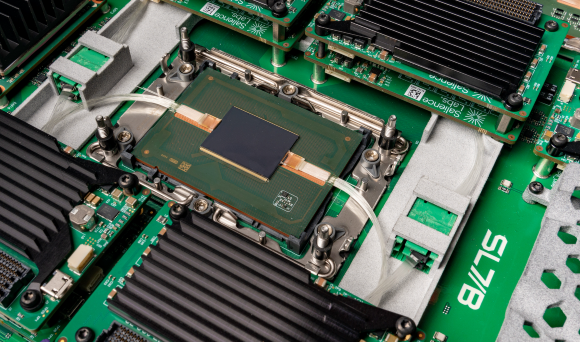
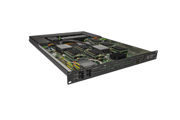
The company describes itself as a specialist in photonic solutions targeting connectivity for AI datacentre infrastructure. The company is building photonics switches for AI infrastructure that solve what it calls “fundamental networking bottlenecks” by enabling all-optical networking between compute nodes. This results in higher-bandwidth and lower-latency connectivity necessary to improve AI Inference workload performance.
A new generation of interconnect
Salience Labs suggests that its all-optical switch solution has the potential to enable a new generation of interconnect network architectures for faster and more efficient AI systems.
“What our users want is a photonic switch to connect their AI clusters that is compatible with existing infrastructure while delivering higher bandwidth, lower latency and power savings. The completion of this round [the company secured $30M Series A funding in 2025] will further our development and help us bring our product to customers to enable not just the savings, but large cluster connectivity,” said Vaysh Kewada, co-founder and CEO of Salience Labs.
The company works on a mantra of optical in, optical switching and optical out – this is to keep the payload fully optical whilst directing data to where it needs to go, thereby (it claims) eliminating the need for expensive transceivers.
Core features
Kewada and team say that the company’s approach achieves a reliable, low-loss optical fabric for fast switching that is compatible with standard links. It offers standard control for deployment and fast switch configuration, temperature/power monitoring and conventional software interfaces.
AI models are data-movement limited, so the Salience switch enables all optical networking between compute nodes, removing bottlenecks. It offers what is said to be “very low latency” as well as high-bandwidth networking for faster job completion at reduced power.
Meet the CEO
CEO Kewada is an ex-IBMer and the Computer Weekly Developer Network (CWDN) sat down with her on a cold February morning to learn more about the way Salience Labs hopes to change the architectural foundations and interconnects of the future computing landscape.
CWDN: Your company’s technology is the result of over 10 years of research into silicon photonics and Salience’s switch is built for AI with a focus on compatibility, reliability and manufacturability… but the current AI renaissance wasn’t really happening a decade ago, are you clairvoyant or did you skew development towards AI in more recent times?

Kewada: We’re building a system-level optical switch specifically for scale-up AI infrastructure, where latency, bandwidth & power economics are fundamentally different.
Kewada: Not clairvoyance – just a clear view of where computing bottlenecks were heading. Even a decade ago, it was obvious that performance scaling was becoming limited by data movement rather than compute. Our early work focused on building reliable, manufacturable silicon photonic switching with low loss and predictable behaviour. As AI workloads emerged and scaled, they exposed exactly the problems we were already solving. What changed wasn’t the technology, but the urgency and clarity of the application. AI simply made inefficient networking impossible to ignore.
CWDN: Many networking solutions for AI still rely on packet switching. Salience has taken a circuit-switching approach – why is that the right choice for AI infrastructure?
Kewada: Packet switching offers flexibility, but it comes with real overhead in the form of buffering, contention, variable latency and power consumption. AI workloads are different — they are highly structured, synchronised and extremely bandwidth-hungry. Circuit switching allows us to establish deterministic, lossless optical paths between nodes with effectively zero added latency, so data flows without congestion or packet processing. You can think of it as the difference between reserving a dedicated high-speed rail line versus routing traffic through busy city streets.
Pluggables & co-packaged optics
As network bandwidths increase, huge investment has gone into moving data efficiently from electrical chips into the optical domain through pluggables and co-packaged optics. Optical switching addresses what happens next, enabling flexible architectures while maintaining a low-latency fabric. That low latency allows the scale-up domain to extend cleanly across multiple racks.
CWDN: When most people think about photonics, they conjure up names like NTT, Broadcom, Intek, Coherent Corp. and Marvell Technology or perhaps Jenoptik Group… how does a start-up compete in this lion’s den?
Kewada: Definitely, those companies are leaders in their domains. However, our advantage is depth in silicon photonics design paired with architectural focus. We’re building a system-level optical switch specifically for scale-up AI infrastructure, where latency, bandwidth and power economics are fundamentally different. That allows us to make design decisions that don’t fit traditional product roadmaps. We also designed for manufacturability and deployment from day one. We see ourselves as complementing the ecosystem, not competing head-on with incumbents.
CWDN: What is genuinely different about Salience’s optical circuit switch compared to other optical switching approaches on the market?
Kewada: What’s genuinely different is that Salience has built a fully integrated optical switching technology that is effectively near-lossless at the system level. By integrating optical gain directly into the switch, we overcome the loss typically associated with silicon photonics and keep the fabric within standard link budgets. That means our switch works seamlessly with today’s pluggable optics and is naturally compatible with future co-packaged optics.
Crucially, we design the system end-to-end to preserve signal integrity, not just minimise loss in isolation. This is critical for AI scale-up domains. The result is an optical switch that can meet the needs of scale-up fabrics… and that can be deployed in AI networks without requiring changes to existing infrastructure assumptions. Lastly, we have developed the technology using volume-capable processes and packaging techniques, ensuring it can scale in volume and achieve a competitive price point.
CWDN: Next-generation AI infrastructure requires flexibility and control to achieve efficiency and scale as AI infrastructure demands continue to grow… How does Salience’s optical switch address these needs?
Kewada: Circuit switching is considered rigid, but that’s only true for optical systems with very long reconfiguration times. AI workloads are highly structured, repeating and synchronised, which makes them well-suited to dynamically established optical circuits. Salience’s switch can rapidly create and tear down optical paths to match workload demand, delivering deterministic bandwidth and latency without packet forwarding overheads. Because latency remains extremely low, this also allows us to scale ML models efficiently across multiple racks rather than being confined to a single enclosure. Unlike packet switching, there is no congestion, buffering or retransmission.
This greatly increases job placement flexibility and hardware utilisation under the most demanding system utilisation fluctuations, which leads to better overall efficiency, power consumption and deployment cost at scale.