Photonics - Scintil: Why AI’s next bottleneck is the network, not the chip

This is a guest post for the Computer Weekly Developer Network written by Matt Crowley, CEO at Scintil Photonics.
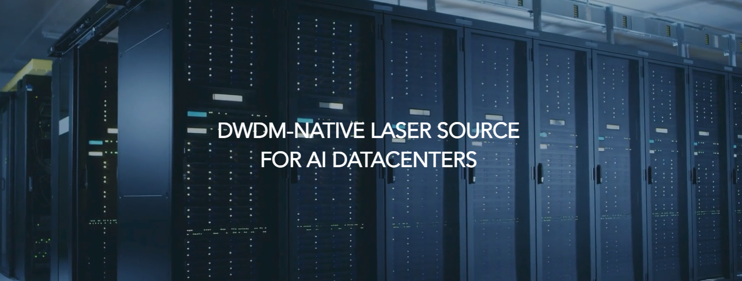
Scintil is known for its work in DWDM laser sources for AI. Using its SHIP™ (Scintil Heterogeneous Integrated Photonics) technology, Scintil developed LEAF Light, the world’s first single-chip DWDM laser source for high-density optical connectivity in scale-up networks.
LEAF Light enables hyperscalers to meet the power, tail latency, utilisation and bandwidth demands of large-scale GPU clusters, leveraging next-generation co-packaged optics (CPO).
Crowley wries in full as follows…
The next gains in AI infrastructure will not come from how fast a single processor runs. They will come from how efficiently processors can work as a networked collective. Emerging architectures make AI processors function not just as a collection of individual devices, but as a unified, memory-coherent supernode spanning thousands of accelerators.
The shift to ultra-high bandwidth network-centric architectures is already underway. To scale AI systems into a supernode of thousands of accelerators, the fabric connecting them is a first-order determinant of usable performance, power density, and cost. Compute is still advancing slowly, but networking now gates how much of that compute can actually be used.
Amdahl’s law says that any system is only as fast as its slowest part. When compute greatly outpaces communications, only speeding up communication will generate significant system improvements.
For infrastructure leaders, that changes the metrics that matter. Energy per bit, latency, bandwidth at the edge, serviceability, and time to volume now belong on the same dashboard as processor performance. The network is no longer supporting infrastructure. It has become part of the performance engine.
Copper’s limits arrived fast
For years, datacentre design followed a practical rule: use copper where it works, and optics where reach requires it. That worked for a time, but as scale-up networks hit the limit in size to span across multiple racks due to copper’s reach and bandwidth constraints, it is time for new networking technology. Optics has reach measured in km and the highest speed copper has reach is measured in cm.
That is why co-packaged optics is moving from an interesting roadmap item to an architectural necessity. Placing optics much closer to the processor or switch die in an integrated package keeps electrical paths inside the package, where only ultra-short reach is needed, and uses optical links for the long reaches that copper cannot handle. The result is a cleaner data path, lower power, and a credible route to far higher bandwidth density.
CPO has already been demonstrated by NVIDIA and Broadcom in scale-out networks with far longer reach than copper and much lower power and higher reliability than pluggables.
More channels per fibre
Co-packaged optics is an important step, but it is not the whole answer. Single channel bandwidth works in the scale-out network because bandwidth requirements are 10 times less than in scale-up networks, and latency is not as critical.
If scaling bandwidth meant scaling a new fibre for every channel, complexity and fibre count would rise fast. Chips only have space for a limited number of fibre attachments, and every fibre attachment adds cost and potential reliability concerns. Dense wavelength-division multiplexing, or DWDM, breaks that pattern by allowing multiple data channels to share the same fibre at different wavelengths, increasing bandwidth without requiring fibre count to rise at the same rate.
The system effect is significant. Fewer fibres reduce congestion in the package, board, and rack. Higher channel counts improve bandwidth density even at lower average channel data rates. Lower per-channel signalling speeds simplify the signal path, remove the need for deep forward error-correction overhead and greatly improve the power efficiency of the link. This is why optics versus copper is no longer a debate. The question now is how to build an optical layer that increases bandwidth density, preserves latency budgets, and can be manufactured in volume.
Recently, a new consortium of AMD, Broadcom, Meta, Microsoft, NVIDIA, and OpenAI announced they would deploy 4 wavelength WDM CPO in scale-up networks, which implies a path to even more wavelengths. This is a watershed announcement in that it makes clear that the only path forward for scale-up networks is optical.
Heterogeneous integration beyond silicon
The industry does not need more laboratory demonstrations of optical performance in isolation. It needs volume-manufacturable technology that can achieve the massive-scale AI datacenters need.
Scale is the real threshold for AI infrastructure adoption. A promising optical design must align with real foundry flows, thermal budgets, packaging constraints, qualification plans, and service models. If it cannot be repeated at volume, it is not yet infrastructure.
That is where the conversation around optical integration becomes specific. The endgame is not simply in having lasers, modulators, or photonic devices; it is in integrating them into a wafer-scale production path that transforms these discrete components into monolithically integrated IP blocks on a fully integrated photonic chip.

Scintil CEO Crowley: Amdahl’s law tells us networks must keep up with system advances elsewhere, or they will end up limiting system performance and scale.
Scintil Photonics is focused on that integration layer. Silicon photonics has been a huge success and without it, the AI datacenter as we know it today would not exist.
But silicon photonics is only half of the story and true integration needs to accommodate the many active components that cannot be made in silicon. Our SHIP™ platform, short for Scintil Heterogeneous Integrated Photonics, is designed to bring non-silicon materials, such as InP for DWDM-native lasers, into established silicon photonics manufacturing flows through foundry-aligned interfaces.
SHIP™ has been validated on Tower Semiconductor’s production platform and is ready for high-volume deployment across Tower’s multi-site global footprint. LEAF Light™ is not only a single-chip DWDM laser source, it is SHIP’s first commercial proof point. LEAF Light™ will deliver the highest per-fibre throughput and densest edge bandwidth reliably at scale.
This is bigger than any single product. AI infrastructure needs an optical integration layer that extends existing roadmaps, works within established standards, and has a clear path to adoption.
The network is a strategic infrastructure
Amdahl’s law tells us that, networks must keep up with advances elsewhere in the system or they will end up limiting system performance and scale.
AI has run up against this limit. When thousands of accelerators must behave like a single superprocessor, the quality of the fabric determines total compute capacity, not the individual accelerators. Optical interconnect technology directly impacts datacenter performance, scale and power efficiency and adoption is a business issue not just a technical one.
But the direction is clear: scalable AI infrastructure will be defined by lower power per bit, higher bandwidth per fibre, tighter latency control, and scalable manufacturing.
That is why this moment matters. The winners in the next infrastructure cycle will not be defined only by better chips. They will be defined by a better total system architecture, and the network now sits at the centre of that decision.